~ Spoorthi Nayak. 10/2015 ~
This tutorial would give an overview of simulating a high-speed I/O transceiver using Cppsim. You would be able to import a channel response, then evaluate the worst case data pattern, and then calculate tap coefficients for Transmitter Pre-emphasis (TXPE), Decision-Feedback Equalization (DFE) and Continuous-Time Linear Equalization (CTLE).
Cppsim is a tool to perform system-level simulations of complex mixed-signal circuits. Systems are specified and simulated within a schematic editor, Sue2, and results are viewed using a waveform viewer (CppSimView or GTKWave).
1 Environment Setup and starting CppSim
Please refer to DFE tutorial on Cppsim website
2 Channel Analysis
The objective of this section is to know how channel behaves. The analysis of channel distortion would help us to determine the different equalization required to restore the signal.
2.1 Importing Project
Download the transceiver library from piazza and place it in the Import_Export directory of CppSim (assumed to be c:/CppSim/Import_Export). Once you do so, start Sue2 by clicking on its icon, and then go to <Tools –>Library Manager> In the Import CppSim Library window that appears, change the Destination Library to transceiver, click on the Source File/Library labelled as transceiver.tar.gz, and then press the Import button. After doing any changes to the libraries in CppSim, restart Sue2. After restarting, select the transceiver library from the schematic listbox. Once the transceiver library is selected, the schematic listbox will show you the list of schematics in the library as shown below.
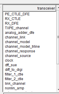
Figure 1: Schematic Listbox
2.2 Schematic Editor
Open channel_response schematic. In the schematics, you will see pulse source and clock blocks. Double click on step_in symbol to change the symbol period and also you could change the clock frequency by double clicking on it. For this tutorial, data rate of 10Gb/s is considered. Symbol period, ts, is set to 1/10e9 and the frequency of the clock is set to 10e9 as shown in Figure 2 and 3. This would generate a pulse of 0.1ns period which is fed into the channel it’s pulse response.

Figure 2: Impulse width setting
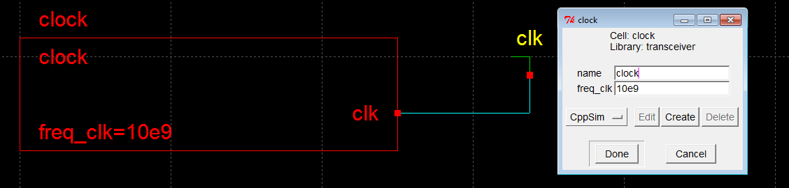
Figure 3: Clock settings
2.3 CppSim Simulation
In the Sue2 schematic window, select <Tools –> CppSim Simulation> from the menu bar. A CppSim Run Menu window similar to the one shown below should open automatically. Note that the Run Menu is already synchronized to the schematic that you will be simulating (channel_response). If this is not the case, click on the Synchronize button in the menu bar, the Run Menu will be synchronized to the schematic in your Sue2 window.
To declare the simulation parameters, click on the Edit Sim File button in the menu. A Emacs window should appear displaying the contents of the simulation parameters file (test.par). The test.par file looks the similar to the contents below:
/////////////////////////////////////////////////////////////
// CppSim Sim File: test.par
// Cell: channel_response
// Library: transceiver
/////////////////////////////////////////////////////////////// Number of simulation time steps
// Example: num_sim_steps: 10e3
num_sim_steps:10e3// Time step of simulator (in seconds)
// Example: Ts: 1/10e9
Ts: 1/1000e9// Output File name
// Example: name below produces test.tr0, test.tr1, …
// Note: you can decimate, start saving at a given time offset, etc.
// -> See pages 34-35 of CppSim manual (i.e., output: section)
output: test// Nodes to be included in Output File
// Example: probe: n0 n1 xi12.n3 xi14.xi12.n0
probe: clk channel_out/////////////////////////////////////////////////////////////
// Note: Items below can be kept unaltered if desired
/////////////////////////////////////////////////////////////// Numerical integration method for electrical schematics
// 1.0: Backward Euler (default)
// 0.0: Trap (more accurate, but prone to ringing)
electrical_integration_damping_factor: 1.0// Values for global nodes used in schematic
// Example: global_nodes: gnd=0.0 avdd=1.5 dvdd=1.5
global_nodes:// Values for global parameters used in schematic
// Example: global_param: in_gl=92.1 delta_gl=0.0 step_time_gl=100e3*Ts
global_param:// Rerun simulation with different global parameter values
// Example: alter: in_gl = 90:2:98
// See pages 37-38 of CppSim manual (i.e., alter: section)
alter:
If you wish to output any other nets in your simulation, you can do it by giving the net a name then adding the name to probe list. To give the net a name click on \net_name in icon listbox and then click on the wire you would like to probe on your schematic, then double click the net_name symbol to enter the name. Once the wire is labelled it can be included in the probe list in test.par file. To save the changes done in Emacs select (Ctrl-x, Ctrl-s). When you are finished, you can close the Emacs window by pressing (Ctrl-x, Ctrl-c). To launch the simulation, click on the menu bar button labelled Compile/Run.
2.4 Potting Results
Double-click on the CppSimView icon to start the CppSim viewer. The viewer should be synchronized to the channel_response cellview which would be shown in the title bar of the CppSim Veiw window. If this is not the case, Sue2 and CppSimView can be synchronized by clicking the Synch button on the left-hand side of the CppSimView window. To view the simulation results, first click on the radio button titled No Output File. After this button is clicked, the output file’s name, test.tr0 will be displayed.
Next, click on the Load button on the left-hand side of the CppSimView window. Once this button is pressed, the Nodes radio button will be filled in, and the probed nodes, as shown below.
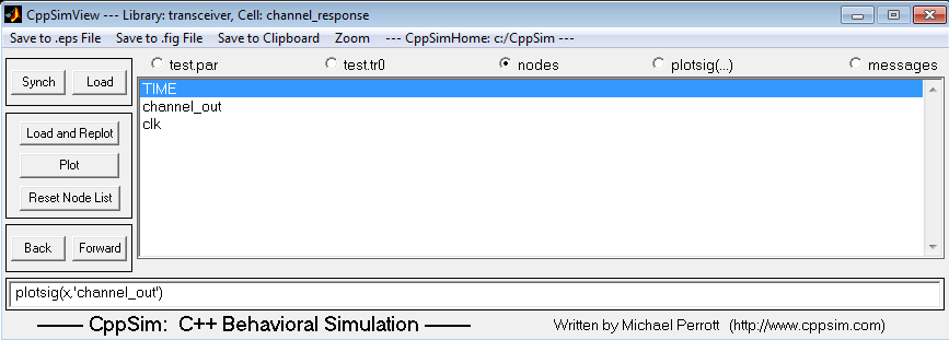
Figure 5: Node List
Double click on the signals channel_out and clock. This will display the channel output plot.
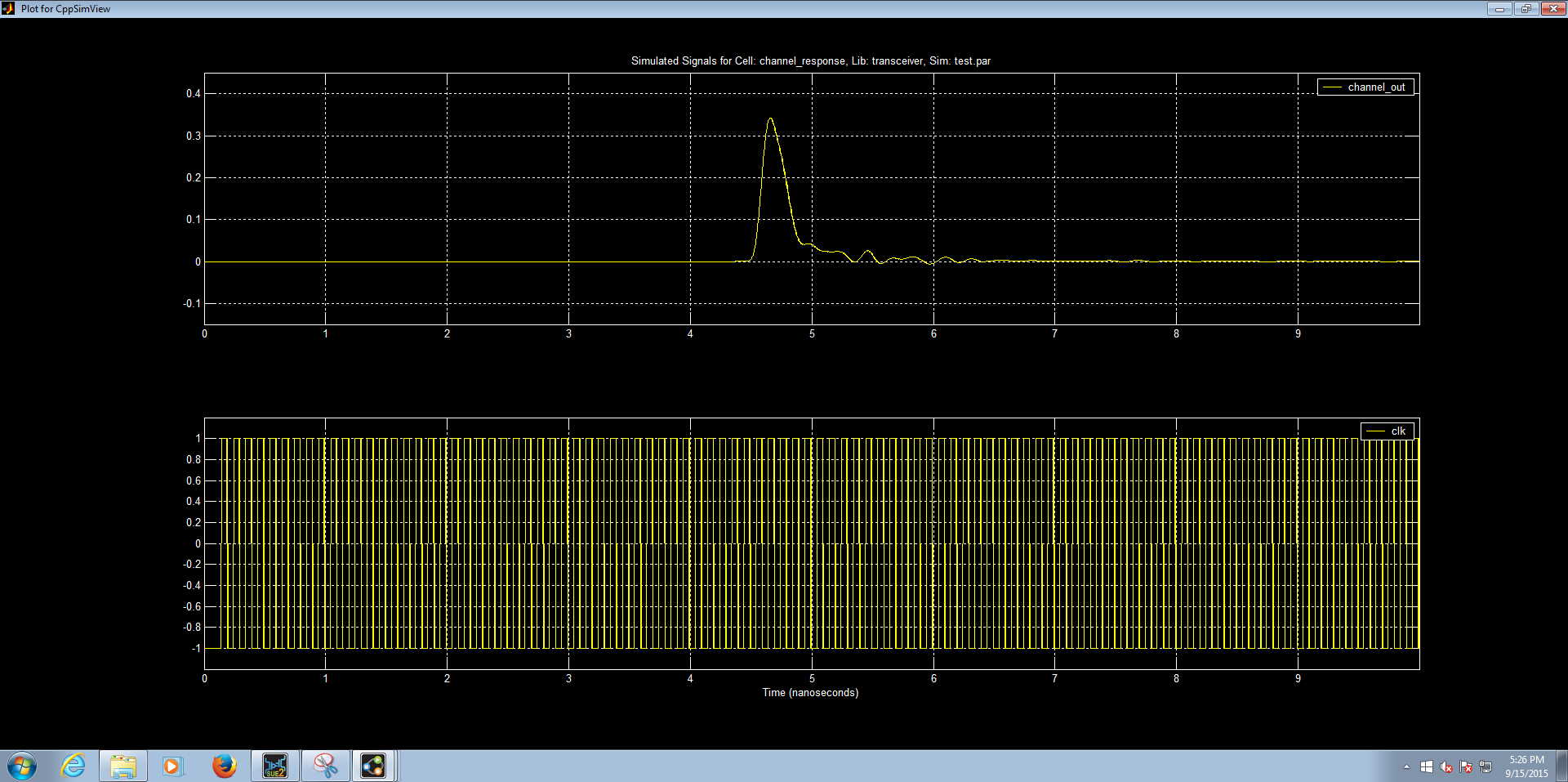
Figure 6: Output plots
To plot channel_out and clk on the same graph, replace ‘nodes’ with ‘channel_out,clk’ in plotsig(x,’nodes’) under plotsig(…) radio button.
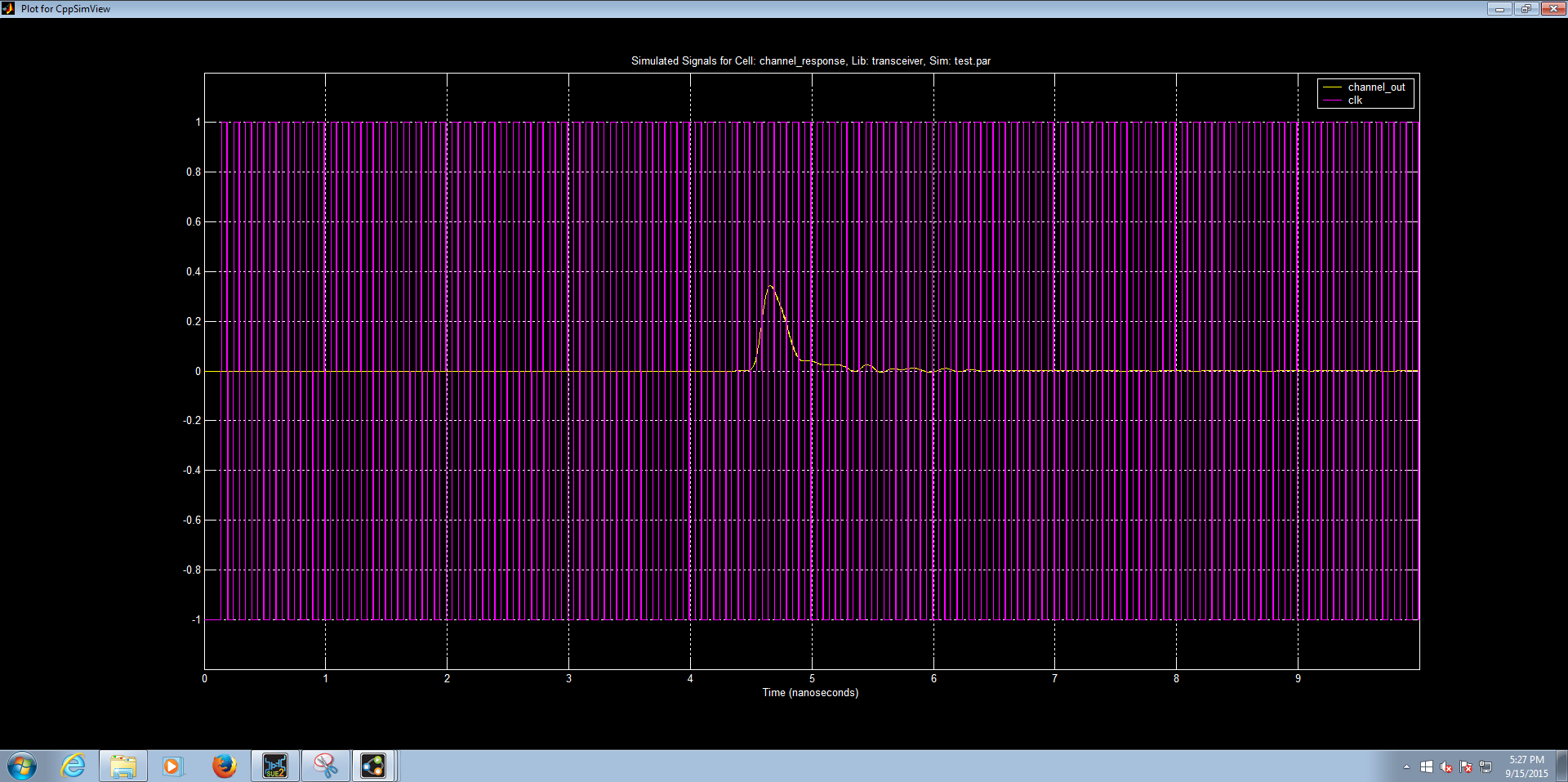
Figure 7: Output graphs on the same plot
A plot window should open displaying both the channel_out and clk signals on the same axis. The purpose of this plot is to determine channel matrix. Channel matrix is obtained by measuring the pulse amplitude at the rising edge of the clk. We can represent the channel response as:
h(k) = […. h(-2) h(-1) h(0) h(1) h(2) ….]
Where h(k) are cursor weight/amplitudes. Channel delay would cause misalignment of clk and pulse, the peak of the pulse needs to be aligned with the the rising edge of the clock. This is done by delaying the clock to account for channel delay. In the schematic the required delay can be entered so that the rising edge of the clk is coincident with the peak amplitude as shown below:
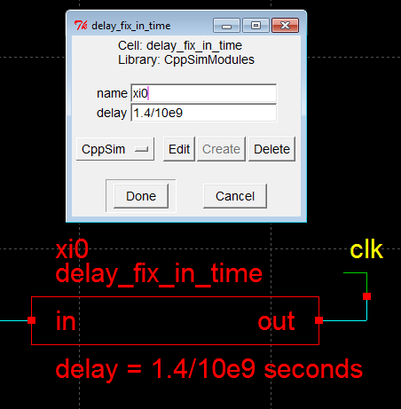
Figure 8: Delay Settings
Click on the zoom radio button at the top of the CppSimView window, and use the (Z)oomX option in the plot window to get a clear view of the pulse.

Figure 9: Zoomed Output Plot
Once the pulse is aligned with the clock, click on the Edit Sim File button in Cppsim window and change the output statement to the following:
output: test trigger=clk
Remove clk from the list of probed nodes by modifying the probe statement. The trigger statement will sample the signals listed in the probe statement only at the rising edge of clk, simplifying the tap weight measurements. After editing the Emacs window, Compile and run the simulation.
To see the individual sample points, click on the (L)ineStyle button at the top of the plot window. The plot window should look something like what is shown below:
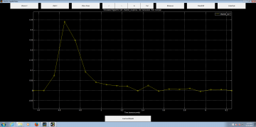
Figure 10: Individual Data points
To measure the amplitude of the sampled values, use the (M)easure button at the top plot window. Click on the first non-zero sample with the left mouse button and then by clicking on the right button the data point value is displayed as shown below:
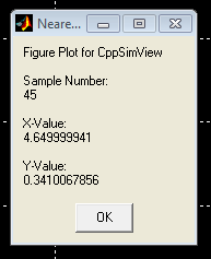
Figure 11: Sample Point Co-ordinates
The amplitude of these non-zero sample forms the channel matrix: h(k) = [0.074 0.34 0.249 0.092 0.041 0.029 ]
Based on the channel matrix we can determine TXPE or DFE tap coefficients.
3 Transmitter Pre-emphasis
The objective of this section is to learn how to calculate the tap-coefficients for TXPE.
For this section of the tutorial use TXPE_channel schematics. This contains Source input, TXPE block and the channel model.
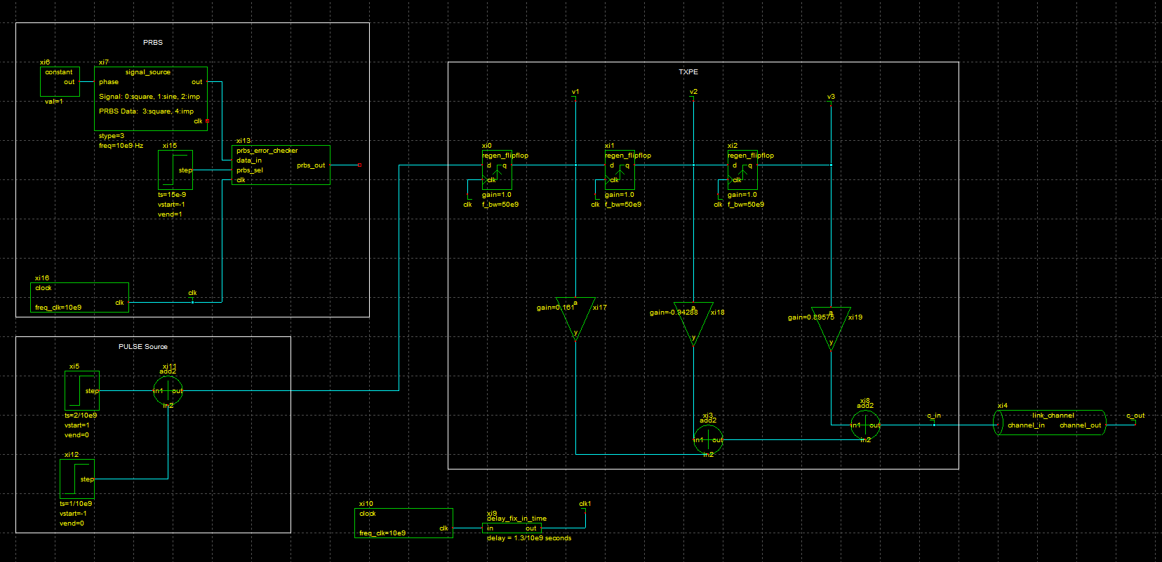
Figure 12: Transmitter Pre-Emphasis
3.1 Calculating Tap Co-efficient
We can represent the channel response as:
h(k) = […. h(-2) h(-1) h(0) h(1) h(2) ….]
To find the tap coefficients with 2 post cursor taps we have:
| y(0) | h(0) | h(-1) | h(-2) | c0 | |||||||
|---|---|---|---|---|---|---|---|---|---|---|---|
| y(1) | = | h(1) | h(0) | h(-1) | c1 | ||||||
| y(2) | h(2) | h(1) | h(0) | c2 |
Y = HC
Where Y is the output vector, H is the channel matrix and C is the tap co-efficient vector. By applying a constrain of Vpp we have:
Cconstrained = [Vpp *C]/sum(abs(C))
By carrying out channel analysis we get channel vector as, h(k) = [ 0.0284 0.313 0.397 0.3615 0.309] (The channel matrix obtained is different from the channel response alone as the components of the TXPE also causes distortion.).
The output vector, y(n) = [1 0 0].
Matlab code:
h=[0.397 0.313 0.0284; 0.3615 0.397 0.313; 0.309 0.3615 0.397];
y=[1 ; 0 ; 0];
h_inv=inv(h);
c=h_inv*y;
c_cont=2*c/(sum(abs(c)))
By using the above equations we can find tap co-efficient for Vpp =2V: Cconstrain= [ 0.89575 -0.94288 0.16137]
Once you calculate the channel coefficients you enter the tap-coefficients in the gain block in TXPE model and run simulations.
For source input you can either use pulse source to see channel ISI effect or use PRBS source to plot the eye-diagram. Refer DFE tutorial for different signal plots. To achieve further improvement in the channel we could increase the number of taps, add CTLE or Decision feedback equalizer at the receiver end.
4 Decision Feedback Equalization
Refer DFE tutorial on CppSim website for this section.
Note: You could use TXPE_channel_DFE schematic in the transceiver library for simulation.
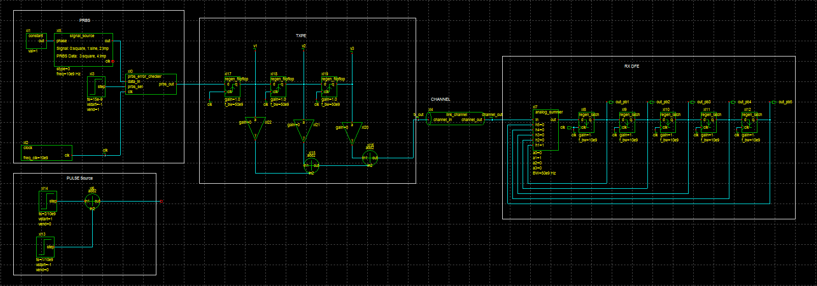
Figure 13: Transceiver Link with TXPE and DFE
5 Receiver Continuous Time Linear Equation
The objective of this section is to know how to implement CTLE.
5.1 CTLE Analysis
RX CTLE is used to boost high frequency components by frequency peaking. High frequency peaking can be used along with amplifier to provide the required gain at the front end of the receiver. The drawback of CTLE is that it amplifies noises and crosstalk along with the signal of interest. Passive RLC components can be used built filter but it is hard to tune and would be PVT sensitive.
CTLE can be modelled using the 2 pole and a zero transfer function:
K would give us the DC gain. fz1 and fp1, fp2 are zero and poles respectively. Peaking range and peaking gain can be adjusted by pole-zero placement.
RX_CTLE schematics shows the implementation of CTLE and PE_CTLE_DFE schematic given contains the schematic of the CTLE integrated along with TXPE and DFE. You could tune the CTLE block to match you link requirement.
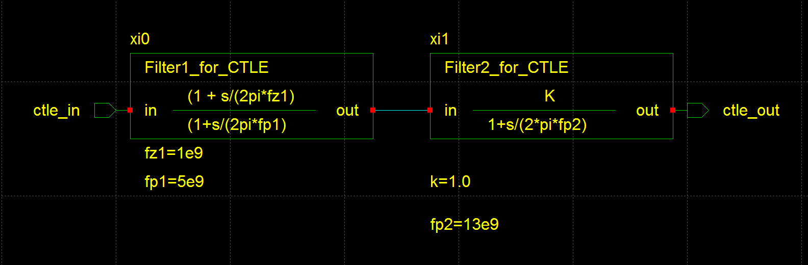
Figure 13: RX CTLE
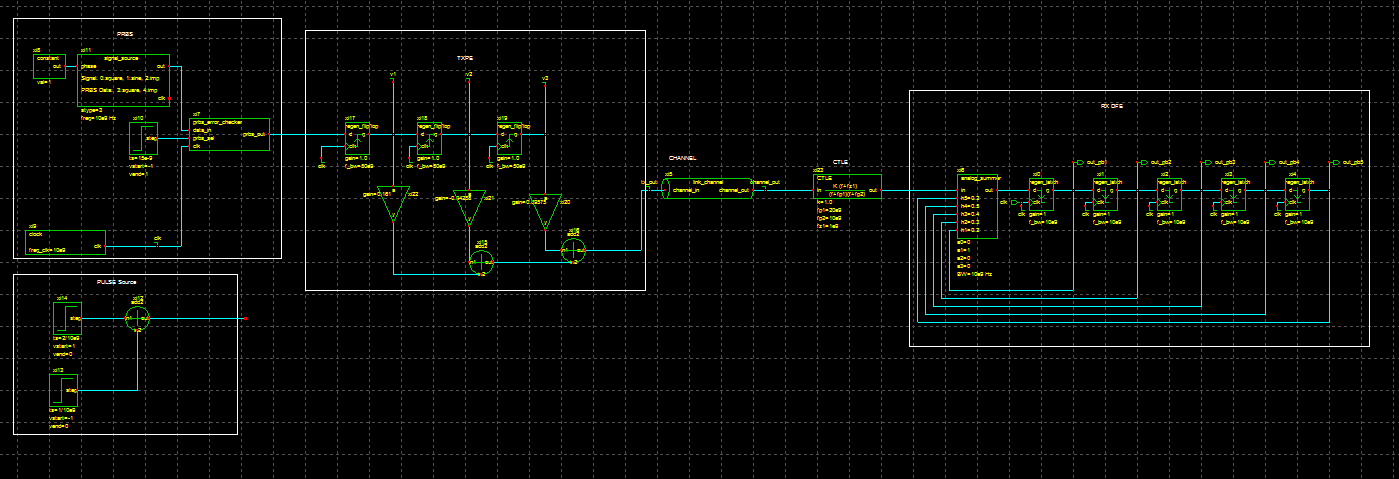
Figure 15: Transceiver Link with TAPE, CTLE and DFE
6 PRBS Generator/Checker
The objective of this section is to learn how to verify the receiver output.
6.1 Using Delay element
One of the ways to check the accuracy of the receiver output is to compare the output of the PRBS generator (transmitter input) with the receiver output. But for this we need to compute the delay of the link and delay the PRBS input to account for channel delay.
6.2 Using PRBS Generator/Checker
In this section we discus a simpler (we could say smarter) way of validating receiver output. Lets look at the a simple 7 bit D-flipflop based PRBS generator. If the initial condition of all the nets is zero, we would not have any output at all! So we could give it a kick start by feeding a one. Then the initial condition of the PRBS generator would be “1000000” and it would start it’s sequence generation from this state. If we had two of identical PRBS generator and both of them had same initial sequence, clock and start time, their outputs would be matched at all times.
Let us assume we have one 7-bit PRBS generator, fully running but we are not sure of its initial state. If we take another PRBS generator open its feedback loop, feed it with output of the first PRBS generator, make sure all 7 bits of the new PRBS generator match the output (state) of the first PRBS generator and then close the loop, the new PRBS generator would be locked with the first PRBS generator as they both have same state. This would mean that their output would be identical. We have now taken one PRBS generator and used its state to initialize another PRBS generator so that they have similar output.
We can extend this to our receiver problem. The receiver output would be PRBS sequence. Our first PRBS generator would be the receiver which would feed in initial condition (state) into a open-loop PRBS generator. Once initial state of all the flip-flops match the sequence order, the loop is closed. This process of feeding initial state is called “seeding”. Close loop PRBS generator would now be synchronized with the receiver output. This PRBS generator could be used for testing the output error of the receiver.
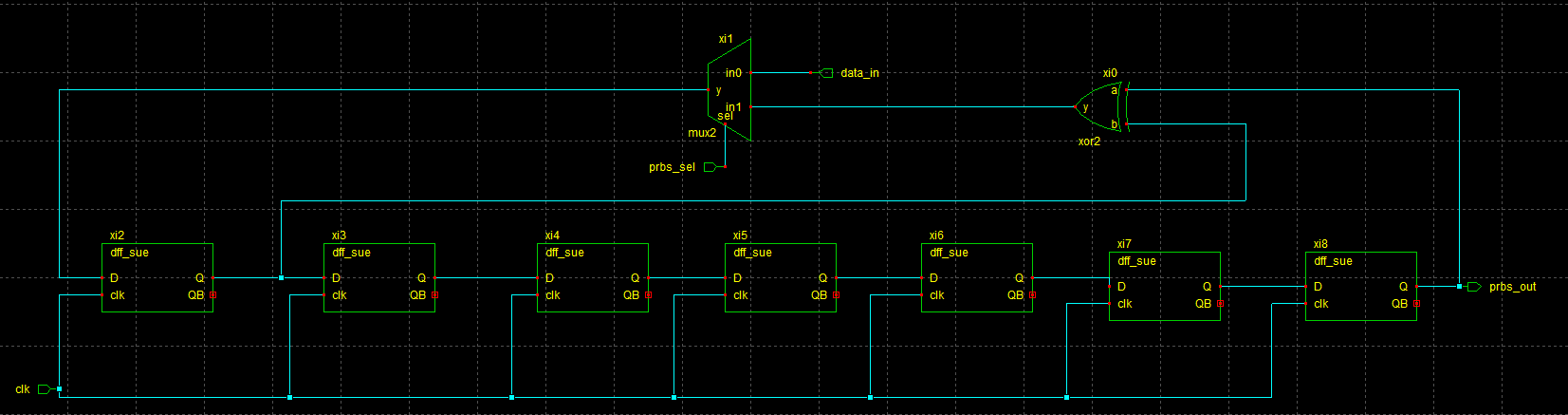
Figure 16: PRBS Generator/Error Checker
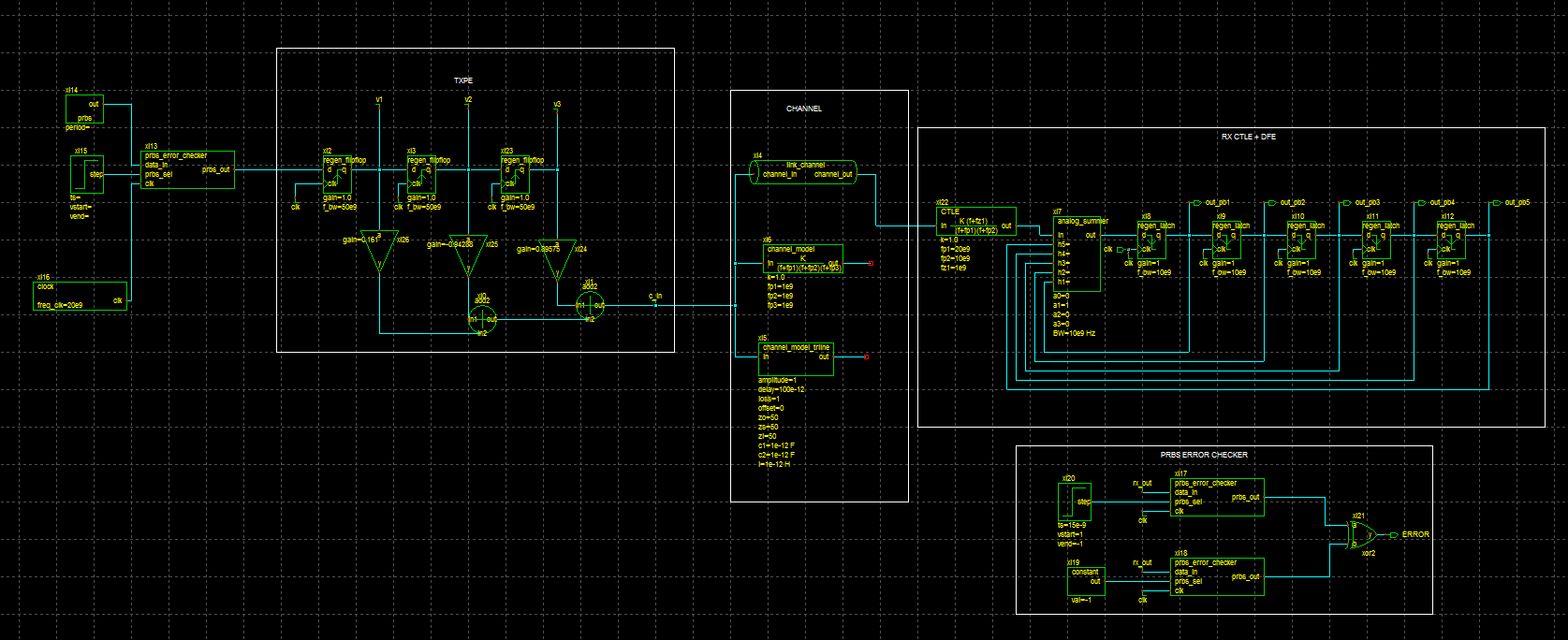
Figure 17: Transceiver with PRBS Error Checker